
|
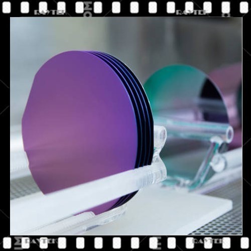
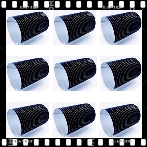
Technical parameters of diode level 3-inch single crystal chip |
Technical parameters of diode level 4-inch single crystal chip |
|
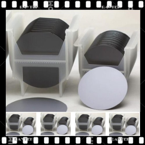
1. Size 1.1 Silicon Wafer Dia. :76.2 +/- 0.4mm 1.2 Bending: ≤0.035mm 1.3 Thickness Tolerance :≤0.03 mm 1.4 Perpendicularity The diagonal lines of the rectangle in the film are equal Tolerance :+/-0.5mm 2. Technical Data 2.1 Conductive parameters :N Type 2.2 Resistivity :5-6OΩ .cm or customized 2.3 Minority-Carrier Lifetime : ≥100 μ s 2.4 Oxygen content : <1.0 ×10¹⁸atoms/cm3 2.5 Carbon content : <5.0 × 10¹⁶atoms/cm3 2.6 Crystal orientation : 111± 1.50 2.7 Dislocation density : ≤3000pcs /cm3 2.8 Thickness:280-305μm |
1.Size
1.1 Silicon Wafer Dia: 100±0.5mm 1.2 TTV: 0.005μm 1.3 Bending: ≤0.030mm 2.Technical Data 2.1 Resistivity: 5-60Ω.cm or customized 2.2 Conductive parameters: N Type 2.3 Minority-Carrier Lifetime: ≥100μs 2.4 Oxygen content: <1×10¹⁸atoms/ cm3 2.5 Carbon content: <5×10¹⁶atoms/ cm3 2.6 Crystal orientation: 111±1.5° |
|
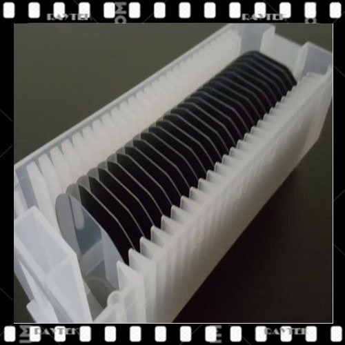
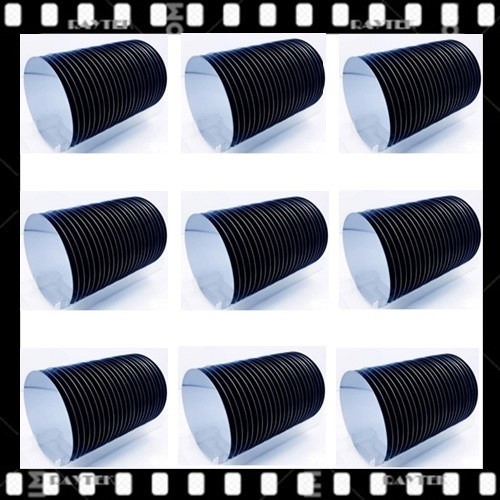
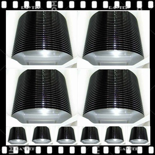
Technical parameters of 6-inch single crystal chip for solar cell |
Technical parameters of 6-inch single crystal chip for solar cell |
|
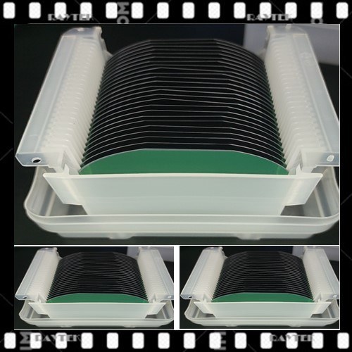
1. Size 1. 1 Silicon Wafer Dia: 160/150±0.4mm 1. 2 Silicon Wafer Width: 125±0.4mm 1. 3 Silicon Thickness: 200/190±20μm 1. 4 TTV: 0.03mm 1. 5 Perpendicularity The diagonal lines of the rectangle in the film are equal Tolerance: ±0.5mm 1. 6 Bending: ≤0.035mm 2. Technical Data 2.1 Resistivity: 0.5-3Ω.cm 2.2 Conductive parameters: N/P Type 2.3 Minority-Carrier Lifetime: ≥10μs 2.4 Oxygen content: <1×10¹⁸atoms/ cm3 2.5 Carbon content: <10×1016atoms/ cm3 2.6 Crystal orientation: (100)±2.0° 2.7 Dislocation density :≤ 1×10³pcs/cm3 |
1.Size
1. 1 Silicon Wafer Dia: 195/200/205±2.0mm 1. 2 Silicon Wafer Width: 156±0.4mm 1. 3 Silicon Thickness:: 200/190±10μm 1. 4 TTV: ≤40μm 1. 5 Perpendicularity: 90°±3° 1. 6 Bending: ≤0.035mm 2. Technical Data 2.1 Resistivity: 0.5-3/3-6Ω.cm 2.2 Conductive parameters: N/P Type 2.3 Minority-Carrier Lifetime: ≥10μs 2.4 Oxygen content:: <1×10¹⁸atoms/ cm3 2.5 Carbon content: <10×1016atoms/ cm3 2.6 Crystal orientation: (100)±2° 2.7 Dislocation density : ≤1×10³pcs/cm3 |
Usa, Uk, Japan, Germany, Spain, France, Swiss, Korea, Russia, Pakistan, India, Portugal, Canada, New Zealand, Australia, Saudi Arab, Turkey, Finland, Poland ,etc.


Raytekoptics Extra value added services offered:
1). Optical workcraft & process solution design;
2). Rough processing raw materials;
3). Semi finishing raw materials;
4). Fabricate custom sizes and shapes;
5). Design and supply custom coatings;
6). Modify and resurface customer supplied materials;
7). Drill holes, notch glass and provide beveled substrates;
8). Precision polish optics with non-standard aspect ratios;
Payment Method: by T/T or Western Union.
Delivery time: 7-10 days.
Quality Warranty: Ruitaiphotoelectric(Raytekoptics) offers quality warranty for our optics products with "3R" policy. For any inferior-quality products, Ruitaiphotoelectric(Raytekoptics) is responsible for return, replacement and refund.


